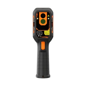
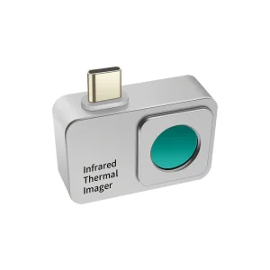
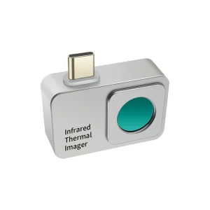
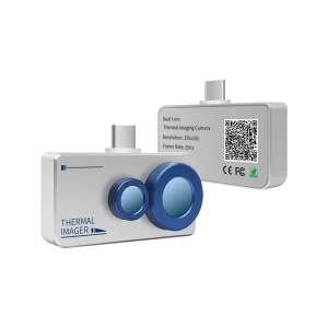
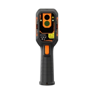
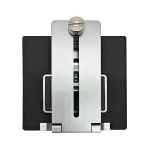
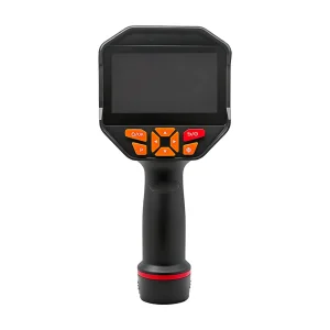
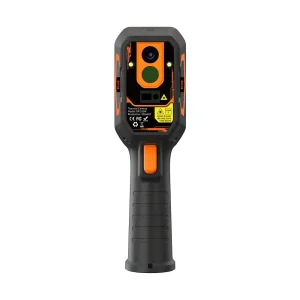
Explore our ODM industrial portfolio, engineered with uncooled VOx microbolometer sensors, radiometric precision, and seamless mobile interface compatibility.
The commercial landscape for infrared sensing has experienced a monumental paradigm shift over the past decade. Historically restricted to high-cost military systems, aerospace defense, and niche heavy-industrial maintenance, thermal imaging technology has democratized into accessible, high-performance compact form factors. Central to this revolution is the ODM Entry-level Mobile thermal imager—a device category that leverages the massive processing power, display capabilities, and connectivity of modern iOS and Android mobile platforms to deliver real-time thermographic diagnostic tools at a fraction of traditional costs.
Key Strategic Takeaway: Mobile thermal imaging transforms smartphones into advanced radiometric diagnostic instruments. Through Original Design Manufacturing (ODM) partnerships, global brands can bypass multi-million dollar R&D cycles and bring compliant, micro-calibrated thermal cameras to market within accelerated timelines.
Entry-level mobile thermal imagers typically combine uncooled Vanadium Oxide (VOx) or Amorphous Silicon (a-Si) microbolometer focal plane arrays (FPAs) with optimized optical assemblies (Chalcogenide or Germanium lenses). By offloading display rendering, user interface processing, thermal palette generation, and cloud connectivity to host mobile hardware via Type-C or Lightning interfaces, these entry-level plug-in accessories drastically lower component counts, weight, and production overhead without compromising essential thermal sensitivity (NETD < 40mK to 50mK).
As global procurement demands shift toward versatile field tools for HVAC troubleshooting, electrical maintenance, building energy loss audits, auto repair diagnostics, and DIY consumer applications, entering the market via a sophisticated Chinese ODM partner provides a decisive competitive edge.
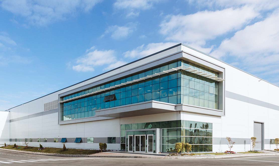
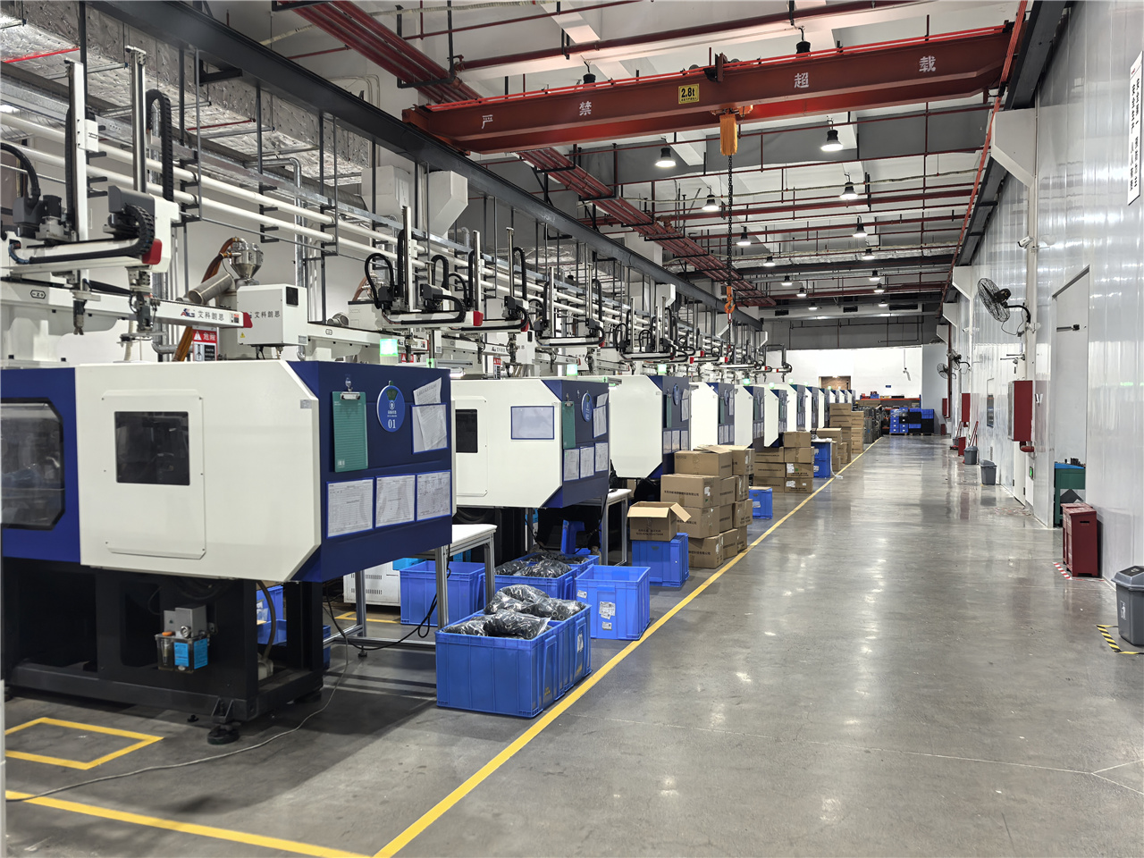
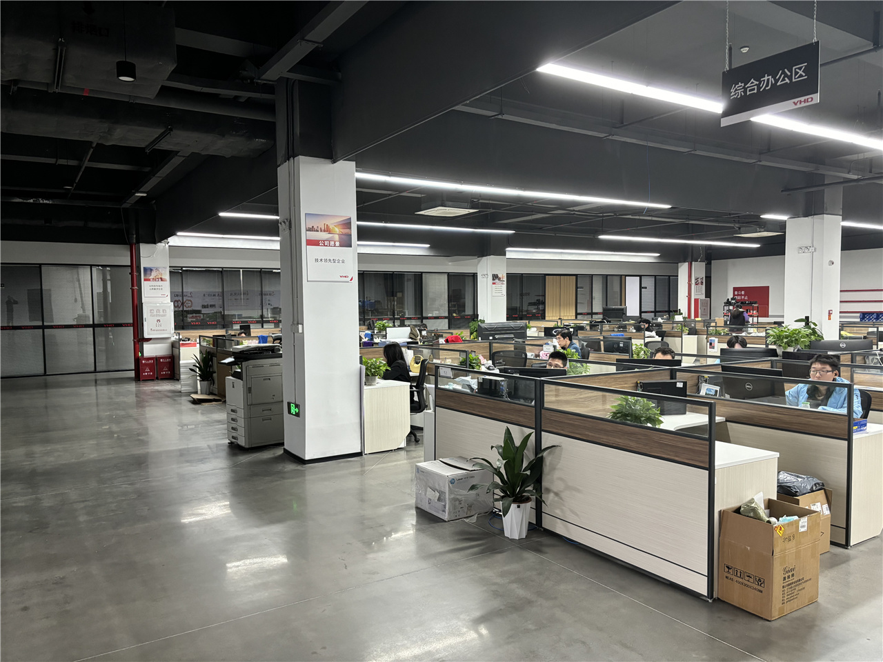
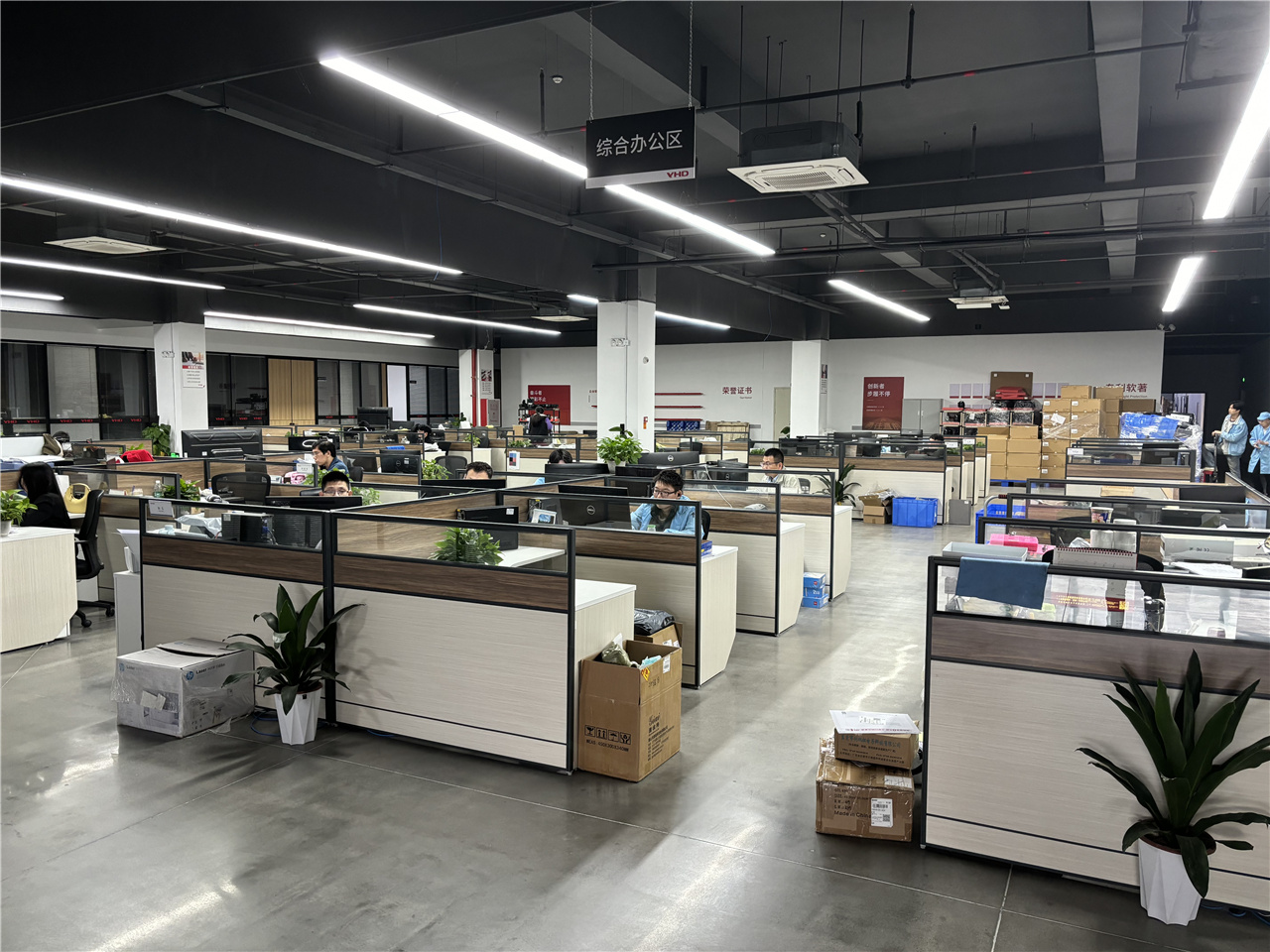
Shenzhen Dianyang Technology Co., Ltd. is a subsidiary of VHD (Shenzhen VHD Technology Co., Ltd.), a publicly listed company on the Shenzhen Stock Exchange. This strategic affiliation gives Dianyang unique access to VHD’s advanced R&D platforms, high-precision manufacturing systems, and rigorous quality management practices—enabling us to deliver thermal imaging products of higher reliability and consistency than typical ODMs.
We specialize in ODM/OEM services for infrared thermal imaging solutions, including handheld thermal imagers, smartphone-connected thermal cameras, thermal analyzers, and thermal imaging telescopes. Our products serve global customers in power inspection, building diagnostics, firefighting, industrial maintenance, and outdoor applications.
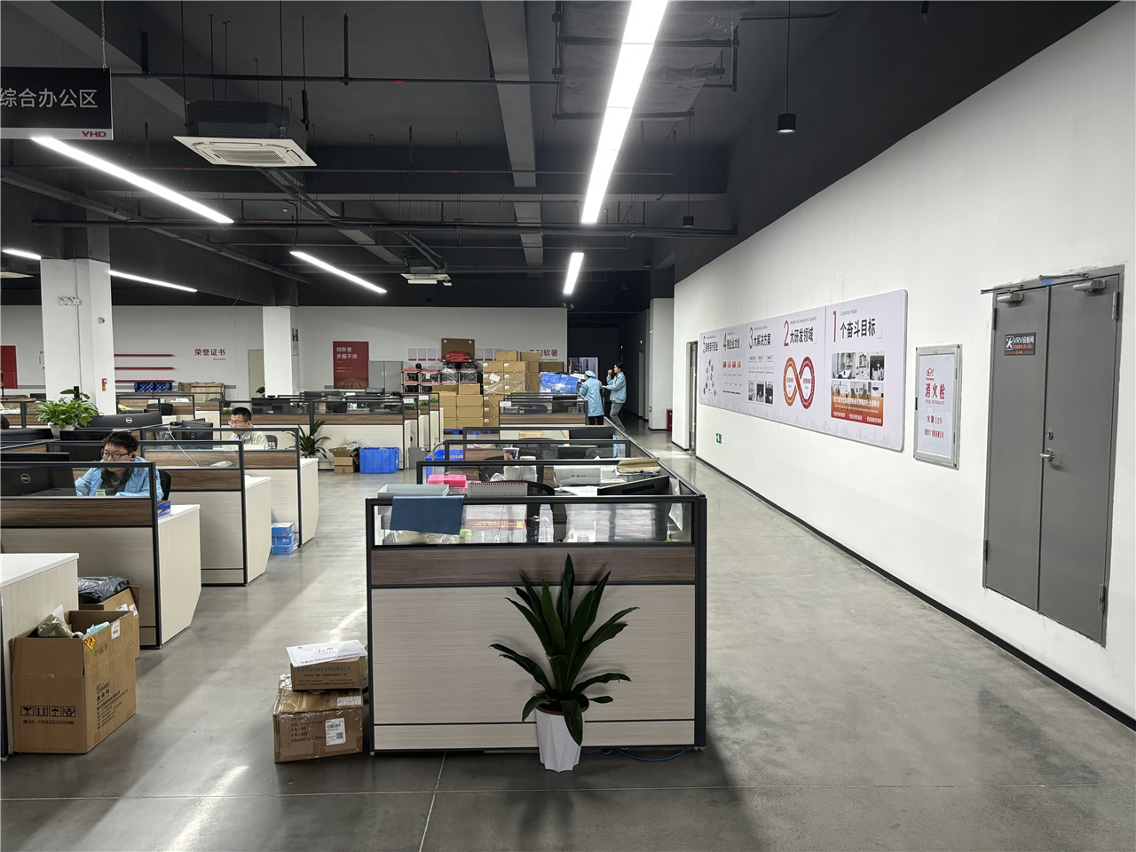
Our dedicated engineering team applies Design for Manufacturing (DFM), Design for Testability (DFT), thermal simulation, and EMC pre-compliance analysis to optimize performance and accelerate development. We also support clients in obtaining key certifications such as CE, FCC, RoHS, REACH, CB, UKCA, KC, and PSE.
Understanding the underlying physics and engineering decisions behind entry-level thermal imaging is critical for enterprise buyers. The entry-level designation does not imply low quality; rather, it reflects optimized resolution tiers (such as 96x96, 120x90, 160x120, and 256x192) paired with efficient optical components designed for volume production.
At the heart of Dianyang's mobile imagers lies an uncooled focal plane array using Vanadium Oxide (VOx) technology. VOx offers a lower Temperature Coefficient of Resistance (TCR) noise floor and superior thermal stability compared to legacy Amorphous Silicon (a-Si). With pixel pitches scaled down to 12µm, optical enclosures are minimized without sacrificing focal plane density.
Connecting a thermal sensor module to a host device requires stringent power control. Dianyang's low-power ASIC architecture limits consumption to <350mW during active sampling. Operating via USB Type-C (UVC protocol) or Apple Lightning, raw radiometric data streams seamlessly to host operating systems without external battery overhead.
Entry-level imagers must deliver precise temperature readings across varying ambient environments. Our systems implement automated Non-Uniformity Correction (NUC) combined with dynamic emissivity adjustment (0.01 to 1.00), target distance compensation, and atmospheric transmission correction engines within native iOS/Android SDKs.
The following matrix details the typical engineering parameters supported across our entry-level mobile thermal imager product spectrum:
| Specification Parameter | DP-09D Series | DP-12D / H1FB Series | H2F6B / DP-25DR Series |
|---|---|---|---|
| IR Resolution | 96 × 96 Pixels | 120 × 90 / 160 × 120 Pixels | 256 × 192 Pixels |
| Pixel Pitch | 17 µm | 12 µm / 17 µm | 12 µm |
| Spectral Range | 8 – 14 µm (LWIR) | 8 – 14 µm (LWIR) | 8 – 14 µm (LWIR) |
| Thermal Sensitivity (NETD) | < 50mK @ 25°C | < 45mK @ 25°C | < 40mK @ 25°C |
| Measurement Temperature | -20°C to +550°C | -20°C to +400°C | -20°C to +550°C |
| Frame Rate Controls | 9Hz (Export License Free) | 9Hz / 25Hz Option | 25Hz Smooth Video Stream |
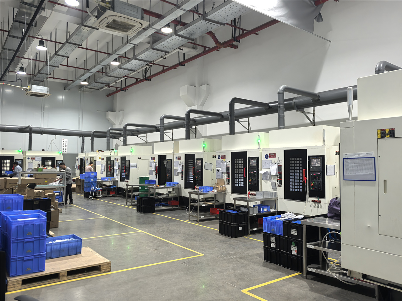
Procuring thermal imaging technology requires an integrated supply chain capable of bridging semiconductor physics, precision optics, surface-mount technology (SMT), and software customization. Located in Shenzhen, Shenzhen Dianyang Technology leverages the world's most dense electronics manufacturing ecosystem.
Traditionally, Germanium lenses accounted for up to 40% of a thermal camera's total cost. By adopting advanced Chalcogenide glass molding and Wafer-Level Optics (WLO) encapsulation, our ODM platforms lower optical manufacturing costs by up to 60% while maintaining crisp 8-14µm transmission efficiency.
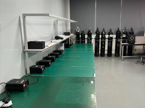
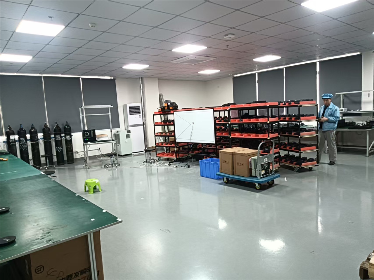
As a subsidiary of publicly listed VHD, Dianyang operates with financial stability, stringent corporate governance, and direct access to heavy-duty SMT lines, automated optical inspection (AOI), and continuous blackbody temperature calibration tunnels.
Our DFM (Design for Manufacturing) and DFT (Design for Testability) methodologies ensure that initial custom housing 3D renders move to T1 sample tooling in as few as 25 business days, accelerating your brand's market launch velocity.
Deploying hardware across international borders requires meeting complex regulatory frameworks, electromagnetic compatibility standards, environmental safety laws, and export licensing rules. Dianyang provides end-to-end certification assistance for seamless global market entry.
All our standard ODM entry-level mobile platforms are engineered to meet CE (European Conformity), FCC (Federal Communications Commission Part 15 Class B), RoHS (Restriction of Hazardous Substances), REACH, CB scheme, UKCA (UK Conformity Assessed), KC (Korea Certification), and PSE (Japan) requirements.
Thermal imaging components above 9Hz are frequently subject to dual-use export regulations. We manage all compliant export licensing documentation in China, offering both 9Hz export-license-free models for frictionless distribution and high-frame-rate (25Hz/30Hz) models for certified commercial applications.
We provide deep SDK customization enabling custom-branded mobile apps (iOS Swift / Android Kotlin) featuring localized UI translation in 18+ languages, customized temperature report templates (PDF/CSV), dynamic color palettes, and cloud backend API synchronization.
Entry-level mobile thermal imagers cater to a diverse array of enterprise and consumer touchpoints. By transforming smartphone screens into high-definition radiometric displays, field technicians and inspectors achieve faster diagnostics.
Identifying overloaded breakers, corroded busbars, loose electrical connections, and failing motor bearings before catastrophic failures occur. Thermographers record radiometric thermal snapshots directly attached to field maintenance work orders.
Detecting thermal insulation voids, structural thermal bridging, moisture infiltration behind drywall, air leakage pathways around windows, and underground radiant floor heating pipe blockages.
Troubleshooting engine misfires, restricted radiator flow, dragging brake calipers, heating core faults, and localized cell overheating within Electric Vehicle (EV) battery packs during fast-charging cycles.
Utilizing high-resolution macro attachments or specialized workbench stands to locate micro-short circuits, failing capacitors, and power management IC (PMIC) overheating on smartphone and computer logic boards.
When partnering with Shenzhen Dianyang Technology for ODM mobile thermal camera development, clients undergo a structured 6-phase engineering workflow designed for maximum quality control, predictable lead times, and risk mitigation.
Defining physical industrial design (ID), connector ergonomics (Type-C extender clearance for phone cases), target thermal resolution, optical FOV (Field of View), and budget constraints.
Executing thermal dissipation simulations to prevent internal heat generation from bleeding into the sensitive microbolometer array, ensuring precise, drift-free thermal readings.
Creating precision injection molds, high-grade CNC aluminum housings, and Engineering Validation Test (EVT) PCBAs. Running initial temperature sensor characterization.
Developing custom application codebases, embedding customized color palettes (Ironbow, Rainbow, White Hot, Black Hot, High Contrast), and tuning radiometric calculation engines.
Running multi-point automated blackbody calibration across ambient temperature chambers (-20°C to +60°C) to generate accurate calibration matrices flashed to onboard EEPROM.
Finalizing CE, FCC, RoHS certifications and commencing automated SMT assembly, mass testing, custom retail packaging production, and worldwide drop-ship logistics.
Get expert answers to common engineering, procurement, software integration, and logistics questions regarding our ODM entry-level mobile thermal imagers.
Our standard Minimum Order Quantity (MOQ) for fully customized ODM mobile thermal imager projects (including custom housing tooling, private-labeled software SDKs, and custom packaging) starts at 500 to 1,000 units. For white-label OEM orders utilizing our standard housing designs (such as the DP-09D, DP-12D, H1FB, or H2F6B series) with custom logo printing, MOQs start as low as 100 units.
Every thermal camera produced by Dianyang undergoes rigorous multi-point temperature calibration inside environmental test chambers using precision reference blackbodies. Our devices feature integrated temperature sensors on the FPA board and intelligent algorithm-driven Non-Uniformity Correction (NUC) to dynamically compensate for ambient temperature drift between -10°C and +50°C, ensuring a measurement accuracy of ±2°C or ±2% of reading.
We provide comprehensive, well-documented Software Development Kits (SDKs) for both Android (Java/Kotlin, C++ NDK) and iOS (Swift/Objective-C). Our SDKs provide direct access to raw YUV frames, temperature matrix tables (radiometric data per pixel), color palette rendering engines, point/line/area temperature measurement APIs, and PDF report generators. Supported OS versions include Android 7.0+ and iOS 12.0+.
Vanadium Oxide (VOx) sensors generally offer lower thermal noise (NETD), superior dynamic range, and faster thermal response times compared to Amorphous Silicon (a-Si) sensors. While a-Si sensors are sometimes cheaper, Dianyang prioritizes VOx technology across most entry-level models to deliver crisp thermal contrast (<40mK sensitivity) and long-term calibration stability for industrial-grade applications.
Thermal cameras operating at frame rates of 9Hz or below are classified as dual-use commercial items and do not require restrictive export licenses for most destinations worldwide. For 25Hz/30Hz high-frame-rate cameras, Dianyang manages all China dual-use export compliance filings, facilitating smooth clearance through international customs for qualified B2B enterprise partners.
Yes. A common field issue with mobile plug-in accessories is interference from thick ruggedized smartphone cases. Our ID design team customizes extended Type-C connectors (up to +4mm to +6mm length) and adjustable silicone gasket spacers to ensure reliable hardware connection regardless of phone case thickness.
Browse our extended product lineup, spanning ultra-portable smartphone attachments to high-resolution handheld diagnostic systems.
 Dianyang