Explore our industrial-grade radiometric thermal imaging devices calibrated for power line inspection, diagnostics, and OEM integration.
Understanding radiometric measurement physics, microbolometer array engineering, and optical sensitivity metrics for industrial procurement decision-makers.
Infrared thermal detection technology has transitioned from specialized aerospace and defense equipment into an essential foundational sensor array across industrial automation, preventive power maintenance, building science, electronics R&D, and consumer health diagnostics. At its core, thermal sensing relies on capturing electromagnetic radiation emitted by object surfaces within the Long-Wave Infrared (LWIR) band, typically ranging from 8 to 14 micrometers (μm). Unlike optical visible-spectrum cameras that measure reflected photon intensities, thermal detection sensors operate independently of ambient lighting, constructing high-resolution thermographic maps based strictly on Planck's Law of Blackbody Radiation and Stefan-Boltzmann's thermal energy output formulas.
In modern commercial and enterprise setups, modern non-cooled microbolometer sensor arrays constructed from Vanadium Oxide (VOx) or Amorphous Silicon (a-Si) represent the industry standard. VOx arrays are widely recognized by systems engineering procurement heads for their superior temperature coefficient of resistance (TCR), yielding dramatically lower Noise Equivalent Temperature Difference (NETD) ratings—frequently under 40 millikelvin (mK) or even 30mK in specialized research instruments. This exceptional sensitivity permits the thermal camera to resolve minute thermal gradient anomalies as subtle as 0.03°C, enabling predictive diagnostic warnings before catastrophic electromechanical breakdowns or PCB electrical trace burnouts occur.
Selecting a high-reliability thermal sensor service and manufacturing supplier demands evaluating several critical engineering metrics that directly govern image clarity, spatial resolution, and radiometric temperature measurement fidelity:
Publicly Listed Exchange Backing, Advanced R&D Engineering Platforms, and World-Class OEM/ODM Thermal Optics Manufacturing.
Shenzhen Dianyang Technology Co., Ltd. operates as a specialized subsidiary of VHD (Shenzhen VHD Technology Co., Ltd.), a publicly listed enterprise on the Shenzhen Stock Exchange. This strategic affiliation provides Dianyang with an unparalleled competitive advantage, granting direct access to VHD's state-of-the-art R&D laboratories, high-precision automated assembly lines, cleanroom optical calibration facilities, and multi-stage quality assurance systems.
Unlike typical contract assemblers or third-party brokers, Dianyang maintains dedicated end-to-end engineering teams specializing in Design for Manufacturing (DFM), Design for Testability (DFT), advanced thermal finite element simulation, and Electromagnetic Compatibility (EMC) pre-compliance testing. This systematic approach guarantees that our full portfolio of handheld thermal cameras, smartphone module imagers, desktop PCB thermal analyzers, and optical infrared scopes achieve top-tier performance consistency, structural durability, and yield rates.
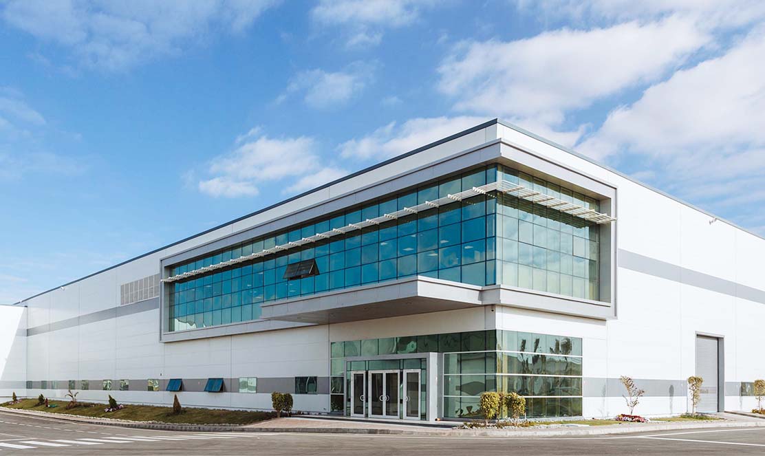
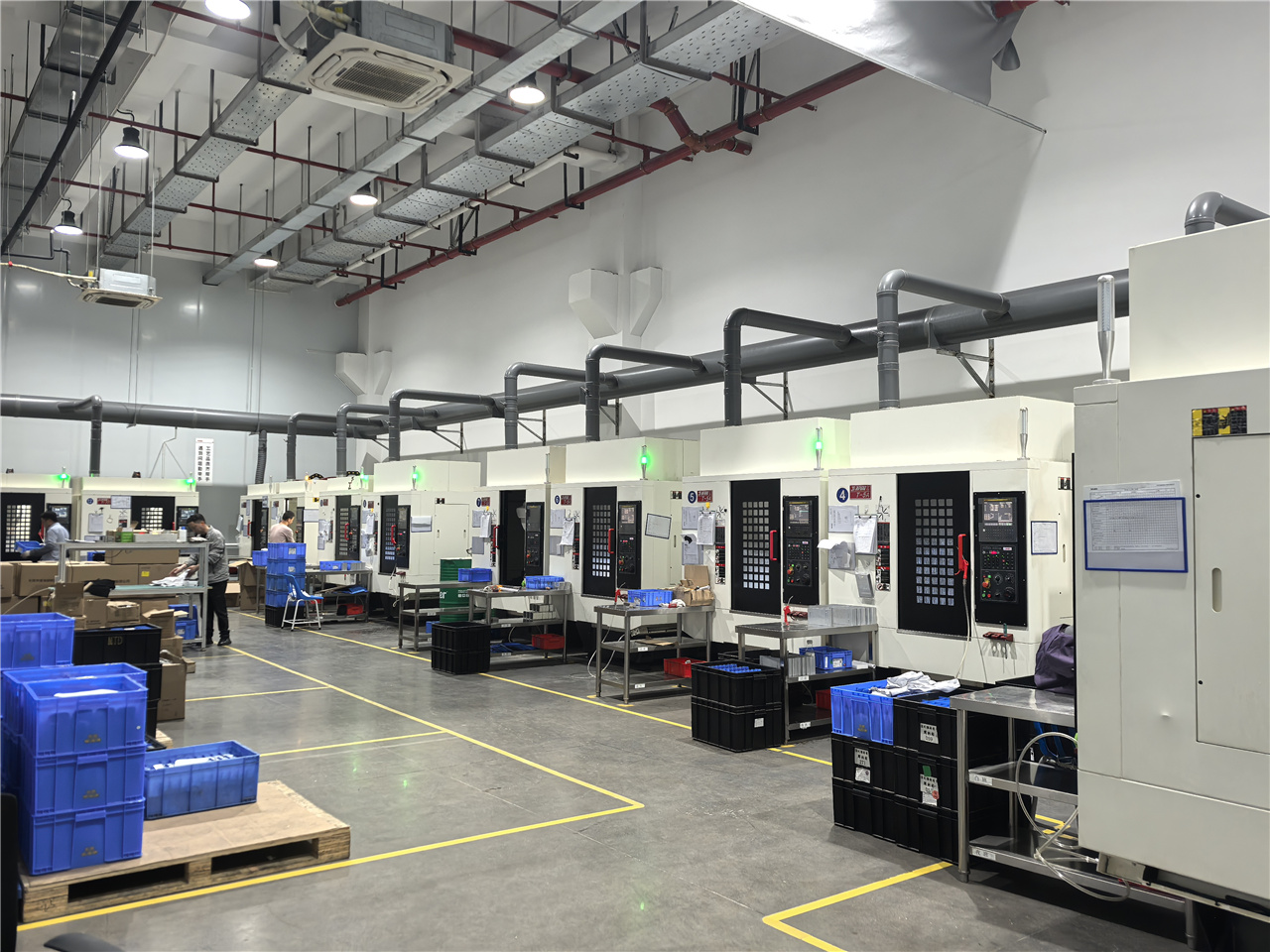
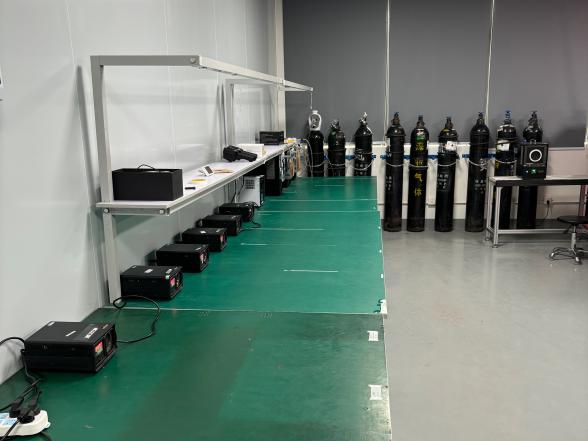
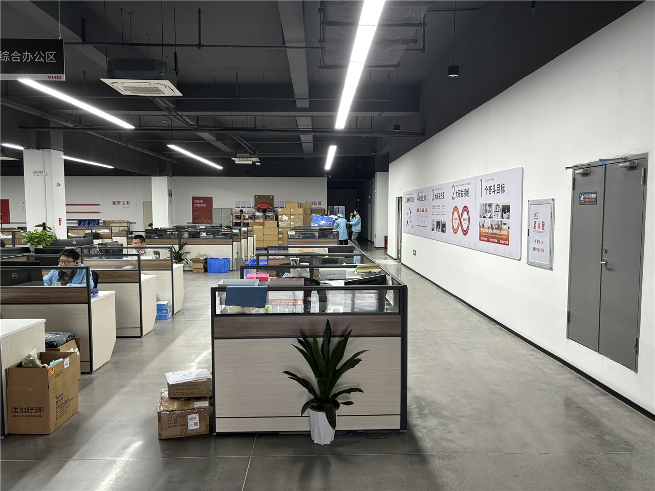
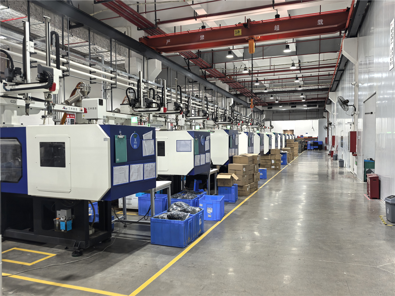
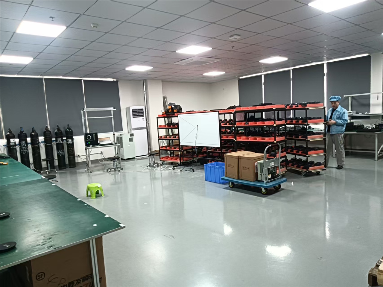
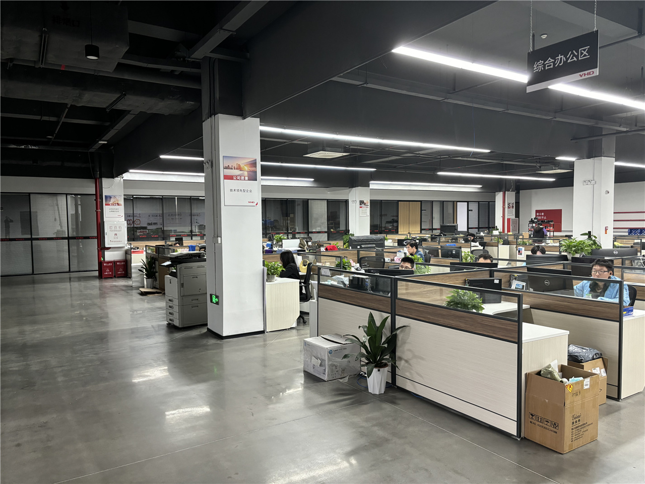
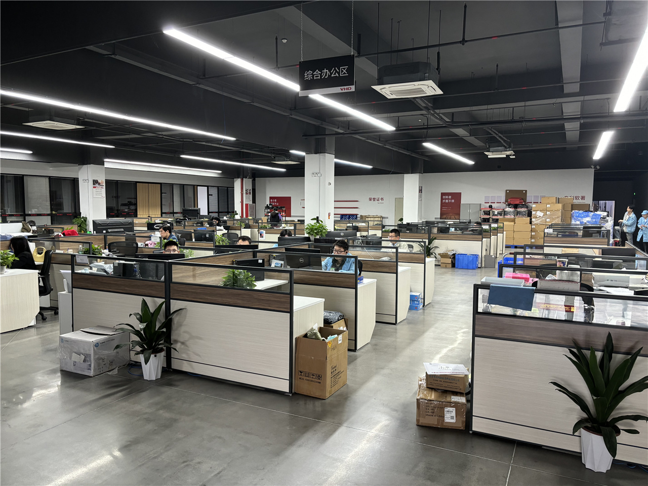
Capitalizing on the world's most integrated optoelectronic cluster for cost performance, rapid prototype iteration, and scalable volume production.
China's domestic semiconductor and optic fabrication network has perfected Wafer-Level Packaging (WLP) and Ceramic Package technologies. This local supply integration lowers raw core procurement lead times by up to 60% compared to traditional European or Western supply lines.
Leveraging Shenzhen’s agile hardware engineering ecosystem, Dianyang transitions client concepts into fully functional, EMC-tested OEM prototypes within 4 to 6 weeks. Our DFM protocol ensures seamless automated production scaling without costly re-tooling delays.
High automated SMT placement rates, localized Germanium (Ge) and Chalcogenide infrared lens processing, and high-volume yield optimization allow us to deliver professional-grade 256×192 thermal cores at a fraction of global competitor cost structures.
How AI integration, miniaturization, and multi-spectral fusion are redefining industrial thermography.
Traditional thermal images can suffer from low spatial edge clarity. Modern sensors combine visible light CMOS cameras with thermal FPAs using real-time edge fusion algorithms (such as Dianyang's Dual-Light spectrum overlay). Embedded Neural Processing Units (NPUs) upscale raw microbolometer data on the fly, highlighting crisp contours for immediate fault identification.
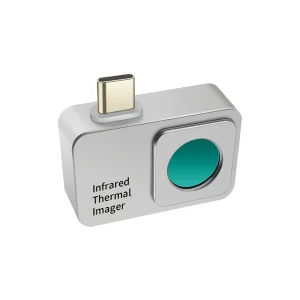
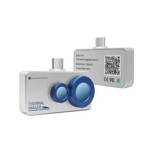
The miniaturization of 12μm pixel pitch VOx cores has spawned ultra-compact plug-and-play thermal cameras (e.g., H2F6B and H2FB series). By offloading display rendering, lithium battery weight, and processing power to host iOS/Android smartphones, these devices bring professional-grade radiometric inspection capabilities to field technicians' pockets.
Static point-and-shoot thermography is rapidly giving way to networked, continuous-monitoring thermal analyzers (such as the CA-30D series). Integrated into factory automation grids via RTSP, Modbus, or MQTT protocols, these fixed thermal sensors provide automated 24/7 alarm triggers whenever component heat surpasses safe operational thresholds.
As manufacturing demands tighter tolerances, modern uncooled microbolometers are pushing the boundaries of thermal resolution. Improved sensor read-out integrated circuits (ROIC) achieve high signal-to-noise ratios, allowing standard industrial cameras to perform precise micro-temperature delta analysis under complex ambient conditions.
From power utility line maintenance to ultra-precise electronic circuit thermal profiling.
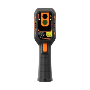
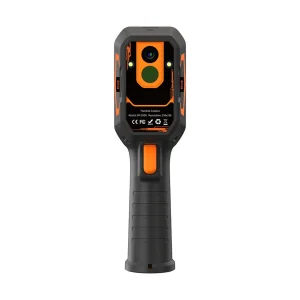
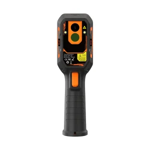
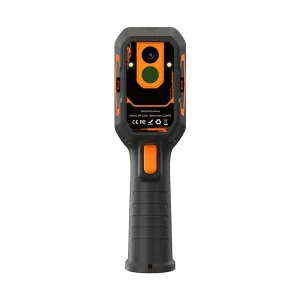
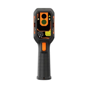
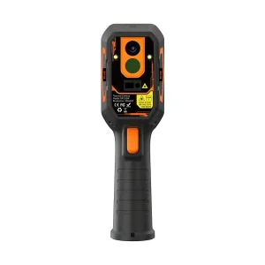
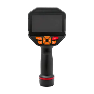
Prevent high-voltage line phase imbalance, loose terminal clamp resistance, and transformer bushing overheat. Handheld models like the DP-12DV and DP-25DV feature laser pointers and dual-light fusion to pinpoint high-resistance loose connections safely from a distance.
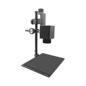
Engineers use specialized analyzers like the CA-30D Thermal Analyzer to map localized component temperatures down to microscopic component levels. It instantly catches short circuits, power management IC overheating, and sub-optimal heatsink contact during product R&D.
Identify hidden insulation deficits, air infiltration gaps, roof moisture intrusion, and underfloor radiant heating tube blockages without destructive physical wall penetration. Thermal imaging reveals precise thermal leaks within seconds.
Detect friction overheating in motor bearings, gearbox failure, misaligned drive belts, and pump impeller cavitation before complete mechanical seizure causes expensive factory downtime.
Deploy elevated skin temperature screening systems for high-throughput public transit hubs, industrial entrances, and healthcare facilities using high-stability radiometric calibration curves.
Equip emergency responders and outdoor professionals with high-frame-rate handheld thermal imagers and thermal monocular telescopes capable of piercing through pitch darkness, dense smoke, and heavy fog.
Direct comparison of resolution, temperature ranges, and application suitability across Dianyang flagship series.
| Model Series | IR Resolution | Spectral Range | Thermal Sensitivity (NETD) | Temp Measurement Range | Special Features | Primary Industrial Target |
|---|---|---|---|---|---|---|
| DP-09D | 96 × 96 | 8 - 14 μm | < 50 mK | -20°C to +300°C | Laser Point Measurement | Basic HVAC & Electrician Tools |
| DP-12D / DP-12DV | 120 × 90 | 8 - 14 μm | < 45 mK | -20°C to +400°C | Dual-Light Vision (DV version) | Power Line & Facility Diagnostics |
| DP-25D / DP-25DR / DP-25DV | 256 × 192 | 8 - 14 μm | < 40 mK | -20°C to +550°C | High-Res Dual Light & Laser Ranging | Industrial Maintenance & Utilities |
| DP-38D | 384 × 288 | 8 - 14 μm | < 35 mK | -20°C to +550°C | LED Night Vision & Pro Radiometry | High-End Plant Audit & Perimeter Security |
| H2FB / H2F6B (Smartphone) | 256 × 192 | 8 - 14 μm | < 40 mK | -20°C to +350°C | Type-C Mobile Direct Plugin / Low Power | Field Technicians & Mobile Audits |
| CA-30D Analyzer | 384 × 288 | 8 - 14 μm | < 30 mK | -20°C to +150°C (Precision) | Macro Circuit Lens & PC Analysis Suite | Electronics R&D & PCB Quality Control |
Essential guidance for international B2B buyers, OEM procurement directors, and distributor partners.
High-resolution desktop thermal analyzers, dual-spectrum tools, and compact smartphone imagers.
 Dianyang