Explore our turnkey thermal imaging devices designed for smartphone integration, industrial non-contact thermography, and high-temperature diagnostic monitoring.
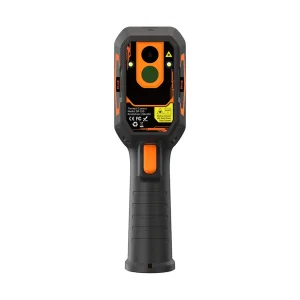
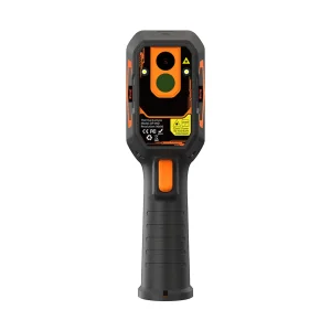
An in-depth guide to microbolometer arrays, thermodynamic measurement algorithms, and custom hardware engineering for modern B2B industrial procurement.
At the core of high-temperature thermal imaging lies the uncooled Focal Plane Array (FPA) microbolometer. Utilizing vanadium oxide (VOx) or amorphous silicon (a-Si) thin films, these sensors measure Long-Wave Infrared (LWIR) radiation from 8 to 14 μm. Precision ODM cameras maintain low Noise Equivalent Temperature Difference (NETD < 40mK or < 50mK), ensuring subtle thermal gradients are clearly visually resolved even when target temperatures exceed 500°C.
Standard thermography struggles with non-linear detector drift when measuring extreme heat. Advanced OEM/ODM high-temperature cameras utilize multi-point blackbody calibration routines. By implementing dynamic emissivity correction tables (ranging from 0.01 to 1.00) and reflected background temperature compensation, these devices deliver reliable measurement accuracy (typically ±2°C or ±2%) across extreme ranges from -20°C up to 550°C.
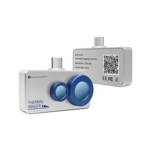
Modern industrial diagnostic platforms combine infrared radiometric sensors with visible light optical modules. Using algorithmically driven spatial alignment, thermal fusion modes (such as MSX or PIP edge enhancement) overlay high-contrast visual detail onto thermal maps. This allows maintenance technicians to pinpoint localized electrical arcing, insulation breakdowns, or mechanical friction instantly.
Key growth drivers, technical demands, and quantitative metrics shaping international trade in industrial infrared thermography.
By partnering directly with specialized Chinese manufacturing exporters, overseas enterprise customers gain access to agile hardware customization. Full-stack ODM engineering encompasses PCB layout redesign, optical lens tuning (standard 3.2mm, 6.5mm, or custom telephoto/wide-angle germanium optics), custom shell injection molding, and proprietary thermal SDK development for desktop and mobile apps.
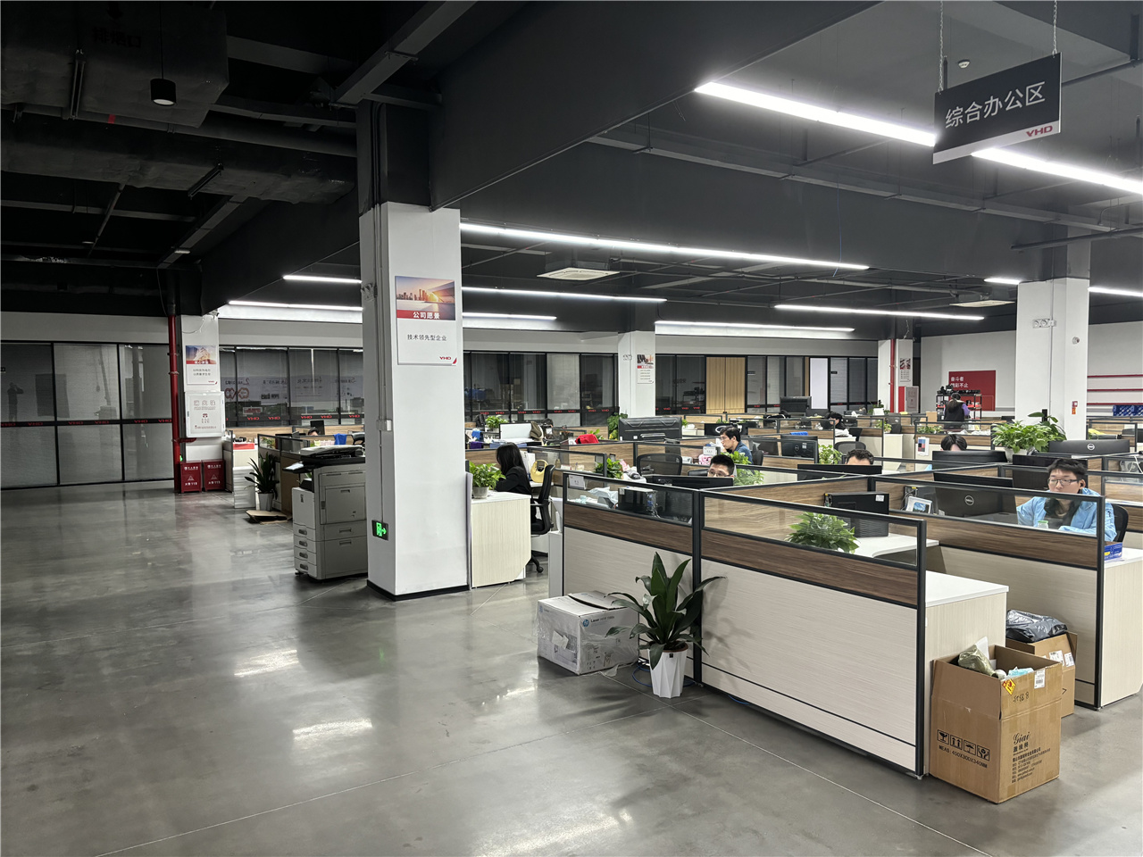
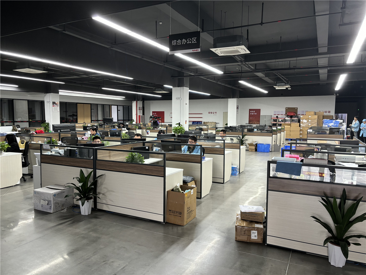
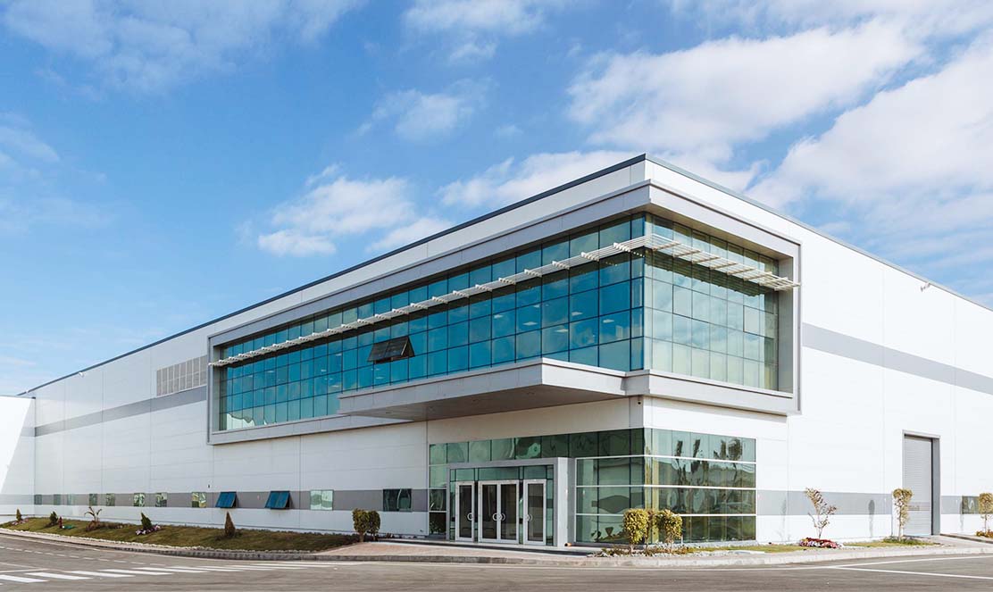
Shenzhen Dianyang Technology Co., Ltd. is a subsidiary of VHD (Shenzhen VHD Technology Co., Ltd.), a publicly listed company on the Shenzhen Stock Exchange. This strategic affiliation gives Dianyang unique access to VHD’s advanced R&D platforms, high-precision manufacturing systems, and rigorous quality management practices—enabling us to deliver thermal imaging products of higher reliability and consistency than typical ODMs.
We specialize in ODM/OEM services for infrared thermal imaging solutions, including handheld thermal imagers, smartphone-connected thermal cameras, thermal analyzers, and thermal imaging telescopes. Our products serve global customers in power inspection, building diagnostics, firefighting, industrial maintenance, and outdoor applications.
Our dedicated engineering team applies Design for Manufacturing (DFM), Design for Testability (DFT), thermal simulation, and EMC pre-compliance analysis to optimize performance and accelerate development. We also support clients in obtaining key certifications such as CE, FCC, RoHS, REACH, CB, UKCA, KC, and PSE.
Targeted solutions engineered for mission-critical environment inspections and precision diagnostics.
Non-contact detection of high-voltage transformers, switchgears, cable splices, and insulator strings. Identify abnormal resistance heat anomalies before catastrophic flashover or power grid failure occurs.
Monitoring refractory lining erosion in steel plants, glass melting furnaces, and petrochemical cracking towers. High-temperature thermal cameras operating up to 550°C prevent wall burn-through and optimize energy efficiency.
Locating hidden moisture accumulation, thermal insulation voids, structural thermal bridging, and HVAC duct leaks. Mobile smartphone-connected units provide fast, portable diagnostic capabilities for building inspectors.
Navigating zero-visibility, smoke-filled structures. High-contrast thermal palettes allow firefighters to locate thermal hotspots, track structural fire spread, and rapidly identify trapped occupants in emergency operations.
To ensure smooth global market entry ("Going Out to Sea"), our engineering and quality assurance teams conduct stringent environmental testing, thermal shock testing, and EMC pre-compliance analysis. We provide full documentation and support for regional standard approvals.
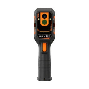
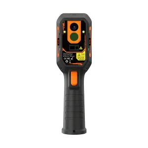
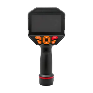
Review our specialized handheld thermal imagers, dual-light optical cameras, and compact high-resolution diagnostic platforms.
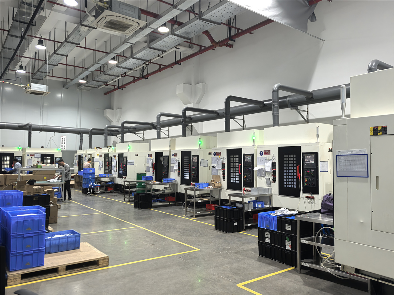
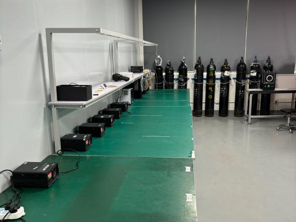
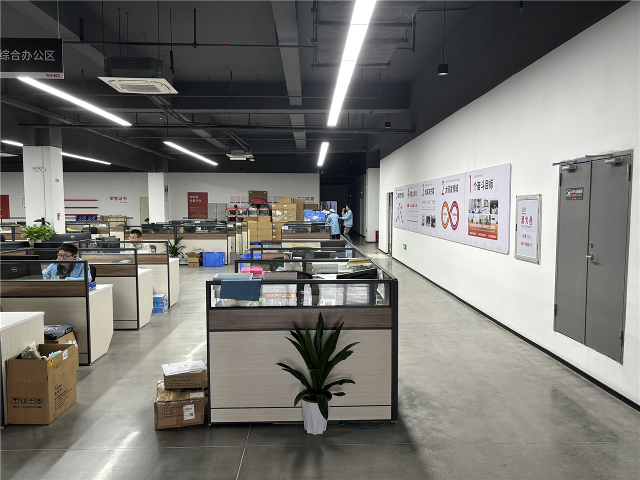
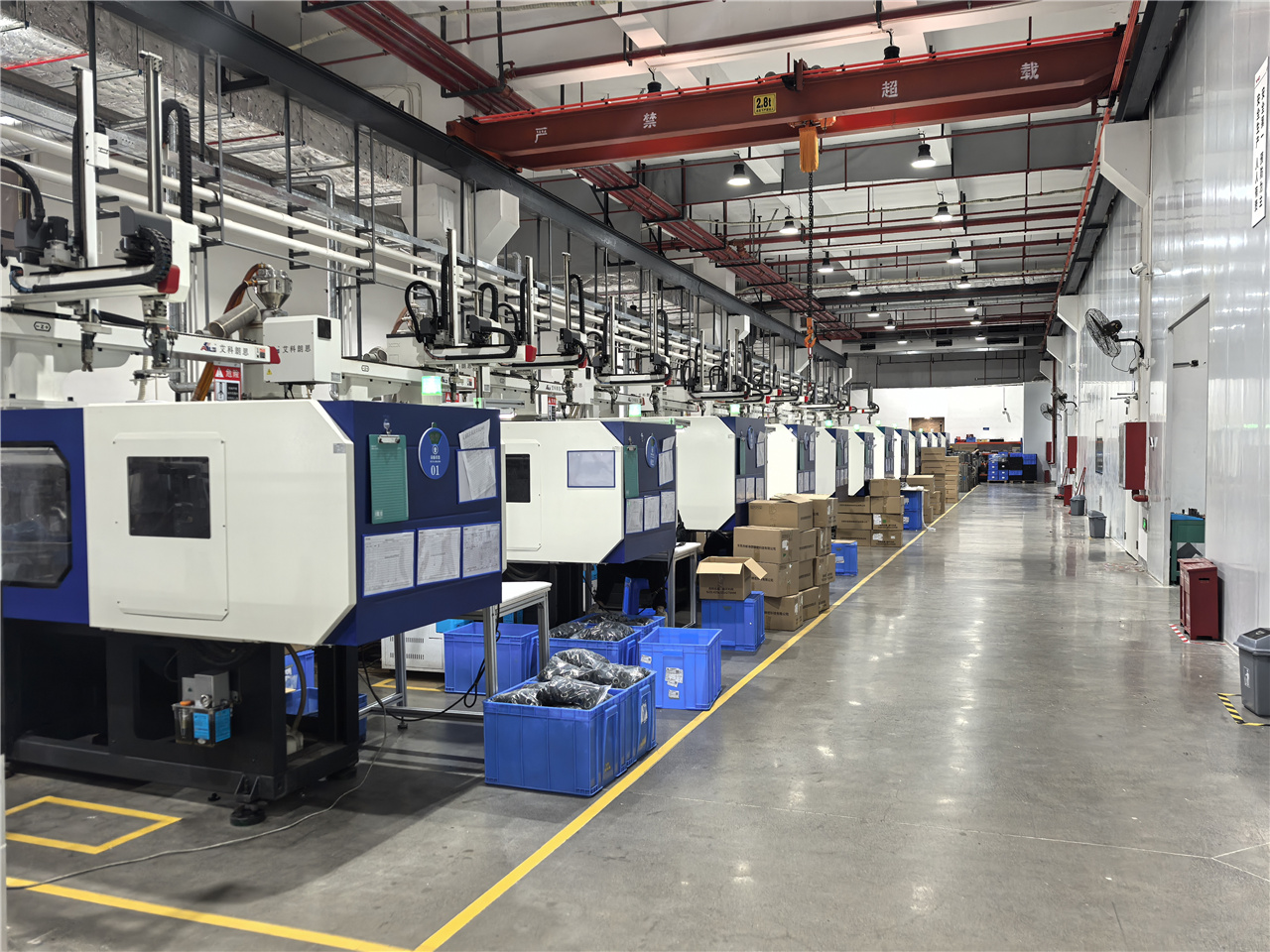
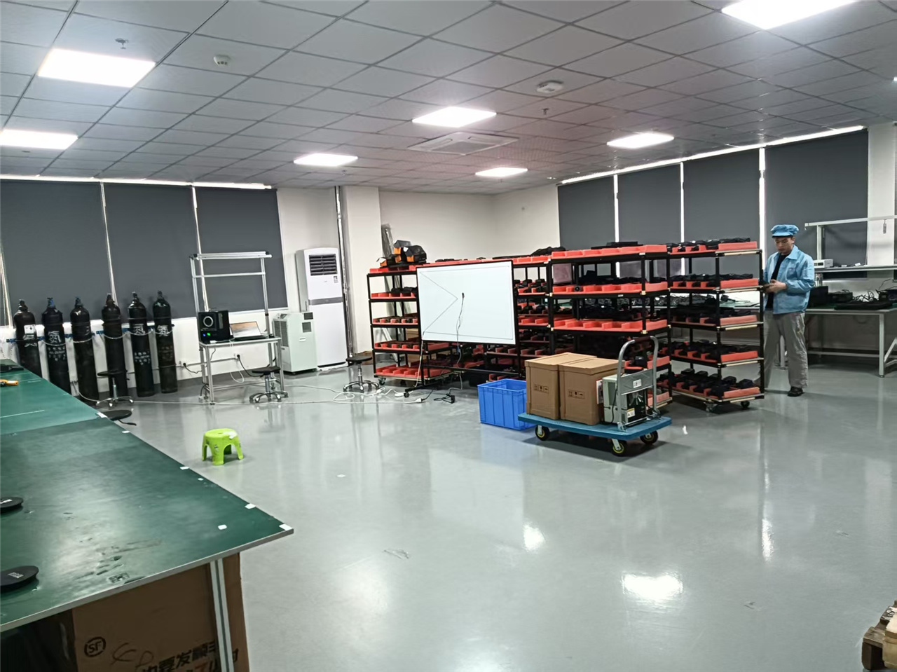
A glimpse into our manufacturing compliance, testing facilities, and international accreditation documentation.
How edge artificial intelligence, IoT miniaturization, and multi-spectral sensors are transforming industrial thermography.
Next-generation ODM cameras incorporate embedded Neural Processing Units (NPUs) directly into the camera core. This allows onboard computer vision models to perform real-time hot-spot classification, fire hazard identification, and automated machinery anomaly scoring without sending raw video streams to external cloud servers.
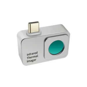
With the rapid adoption of compact Type-C connected infrared modules (such as the H2FB and H2F6B series), mobile thermal imaging turns smart devices into professional diagnostic tools. Global B2B buyers are increasingly leveraging these plug-and-play modules for scalable technician field deployment.
Moving from entry-level 96x96 and 160x120 resolutions up to 256x192 and high-end 640x512 formats (like DP-64D), microbolometer pixel pitch is shrinking to 12μm. This yields sharper thermal contrast, wider field of view (FOV), and improved distance-to-spot ratios (D:S) for safer high-temperature monitoring.
Comprehensive answers regarding high-temperature thermal imaging ODM services, technical specifications, and factory export procedures.
 Dianyang