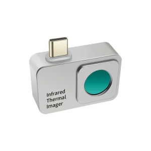
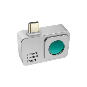
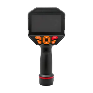
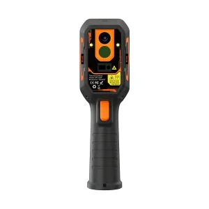
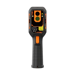
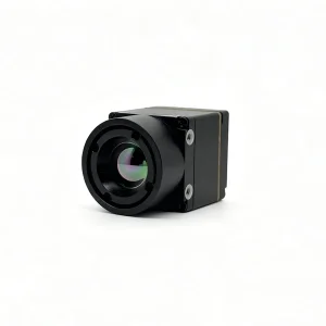
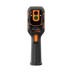
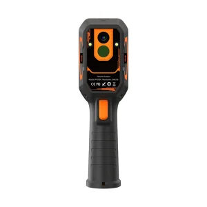
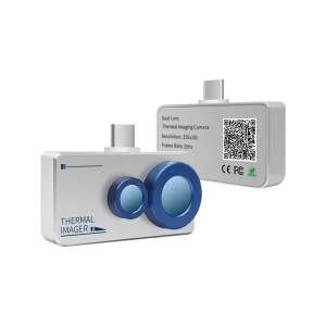
Industrial-grade handheld cameras, mobile attachments, and thermal imaging cores engineered with precision IR optical glass.
In the modern optoelectronics paradigm, thermal imaging glass represents the structural backbone of long-wave infrared (LWIR, 8–14 µm), mid-wave infrared (MWIR, 3–5 µm), and short-wave infrared (SWIR, 0.9–1.7 µm) optical systems. Unlike traditional visual-spectrum glass optics fabricated from fused silica or crown glass, thermal optical media must exhibit exceptional transmissive properties across invisible infrared wavebands where atmospheric absorption windows remain open.
As global automation, defense modernization, smart grid maintenance, and automotive Advanced Driver Assistance Systems (ADAS) accelerate, procurement directors and optical engineers face increasing friction regarding raw material availability, precision diamond machining tolerances, thermal drift management ($dn/dt$), and optical coating resilience. A customized thermal imaging glass supplier must offer more than simple machining; it requires end-to-end material synthesis, single-point diamond turning (SPDT), chalcogenide glass precision molding (PGM), and rigorous surface metrology.
Information Gain Perspective: Mono-crystalline Germanium (Ge) has historically dominated LWIR refractive optics due to its high refractive index ($n \approx 4.00$) and low chromatic dispersion. However, its high thermal refractive index coefficient ($dn/dt = 3.96 \times 10^{-4} /\text{K}$) subjects uncooled infrared cameras to severe defocusing across operational ambient shifts (-40°C to +85°C). Next-generation optical engineering relies heavily on Chalcogenide glass formulations (e.g., $Ge_{28}Sb_{12}Se_{60}$ or $As_{40}Se_{60}$), which feature significantly lower $dn/dt$ values ($30 \times 10^{-6} /\text{K}$), enabling passively athermalized lens assembly designs without complex mechanical focus compensation mechanisms.
Selecting the optimal infrared substrate demands a rigorous trade-off analysis between spectral transmission window, refractive index, dispersion (Abbe number $V_d$), mechanical hardness, density, and thermal expansion properties.
| Substrate Material | Spectral Transmission Range (µm) | Refractive Index ($n$ @ 10µm) | Thermal Coefficient ($dn/dt \times 10^{-6}/\text{K}$) | Knoop Hardness (kg/mm²) | Primary Industrial Application |
|---|---|---|---|---|---|
| Germanium (Ge) | 2.0 – 14.0 | 4.003 | 396 | 780 | High-resolution defense optics, LWIR thermal cores, dual-band systems |
| Chalcogenide Glass (IRG25/BD2) | 1.0 – 12.0 | 2.498 | 34 | 150 | High-volume molded automotive ADAS, passive athermal lens systems |
| Zinc Selenide (ZnSe) | 0.6 – 20.0 | 2.406 | 61 | 105 | High-power CO2 laser windows, medical thermal diagnostic devices |
| Silicon (Optical Si) | 1.2 – 7.0 | 3.418 (at 4µm) | 160 | 1150 | MWIR imaging sensors, drone surveillance payloads, lightweight optics |
| Zinc Sulfide (ZnS - Cleartran) | 0.4 – 12.0 | 2.200 | 43 | 230 | Multispectral airborne reconnaissance, FLIR sensor domes |
Thermal imaging glass components serve as the critical interface between chaotic real-world thermal radiation environments and delicate uncooled focal plane arrays (FPAs) or vanadium oxide (VOx) / amorphous silicon (a-Si) microbolometer detectors.
High-voltage electrical substations require continuous non-contact temperature surveillance. Thermal optics customized with narrow field-of-view (FOV) telephoto Chalcogenide lenses enable inspection cameras like the DP-25DR and DP-64D to spot micro-Kelvin temperature anomalies across high-tension power lines from safe standoff distances.
Automotive vision in zero-visibility conditions (dense fog, blizzard, heavy smoke) demands far-infrared (FIR) sensing. Precision glass-molded Chalcogenide optics coupled with Diamond-Like Carbon (DLC) exterior coatings provide environmental survivability against gravel impacts while projecting crisp thermal signatures to AI perception algorithms.
Miniaturized thermal imaging attachments, including the H1FB and H2FB series for smartphones, integrate wafer-level optical glass assemblies. They allow field inspectors to quickly detect HVAC airflow leakages, structural thermal bridging, moisture ingress beneath roofing membranes, and latent electrical overload points.
Machine vision setups utilizing embedded modules like the MD-64CA Thermal Imaging Module rely on specialized optical windows and fixed-focus thermal glass optics to monitor temperature distributions during automated plastic injection molding, laser welding, and semiconductor packaging.
Fabricating high-performance custom thermal imaging glass requires strict process control across raw element purification, glass melting, optical blank slicing, grinding, single-point diamond turning (SPDT), and thin-film vacuum deposition.
1. Single-Point Diamond Turning (SPDT) & Precision Molding
For complex aspheric and diffractive surface profiles, SPDT utilizes ultra-precise natural diamond cutting tools mounted on air-bearing spindles. This achieves surface roughness ($Ra$) values below 3 nanometers and form accuracy ($\text{PV}$) better than $\lambda/4$ at 632.8nm. For high-volume production, Precision Glass Molding (PGM) heats chalcogenide glass blanks to their glass transition temperature ($T_g \approx 180^\circ\text{C} - 350^\circ\text{C}$), pressing them into high-durability tungsten carbide molds to yield finished aspheric lenses without polishing.
2. Advanced Thin-Film Coatings (AR & DLC)
Uncoated Germanium reflects roughly 36% of incident infrared radiation per surface due to its steep refractive index ($n = 4.0$). To maximize signal-to-noise ratios (SNR), our optical thin-film physics team utilizes physical vapor deposition (PVD) to apply custom coating stacks:
The global demand for custom thermal optics is experiencing unprecedented growth driven by commercial price accessibility and multi-industry adoption. Key structural shifts in global procurement include:
Demand centers heavily on high-resolution industrial monitoring, predictive maintenance, and strict compliance with local regulatory guidelines (CE, FCC, RoHS, REACH). Buyers prioritize supplier transparency, rapid thermal simulation validation, and verifiable MTF performance data.
Rapid expansion in smartphone-integrated thermal sensors (e.g., H1FB, H2FB, H2F6B models) and commercial security infrastructure driving demand for low-cost molded chalcogenide optical elements manufactured at scale.
Shenzhen Dianyang Technology Co., Ltd. is a subsidiary of VHD (Shenzhen VHD Technology Co., Ltd.), a publicly listed company on the Shenzhen Stock Exchange. This strategic affiliation gives Dianyang unique access to VHD’s advanced R&D platforms, high-precision manufacturing systems, and rigorous quality management practices—enabling us to deliver thermal imaging products of higher reliability and consistency than typical ODMs.
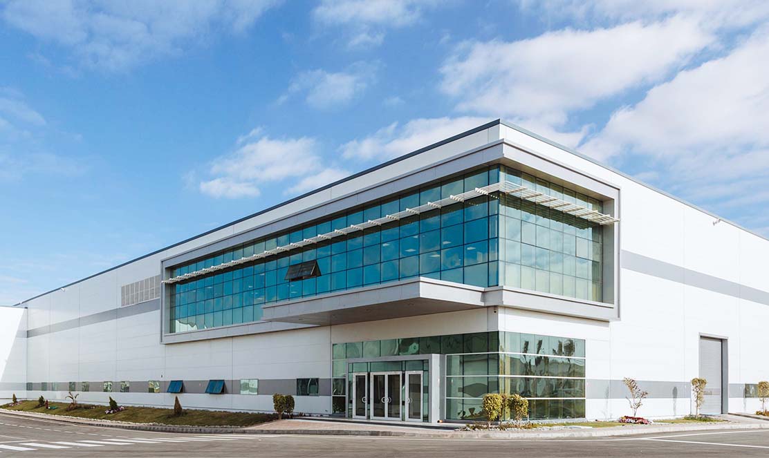
We specialize in ODM/OEM services for infrared thermal imaging solutions, including handheld thermal imagers, smartphone-connected thermal cameras, thermal analyzers, and thermal imaging telescopes. Our products serve global customers in power inspection, building diagnostics, firefighting, industrial maintenance, and outdoor applications.
Our dedicated engineering team applies Design for Manufacturing (DFM), Design for Testability (DFT), thermal simulation, and EMC pre-compliance analysis to optimize performance and accelerate development. We also support clients in obtaining key certifications such as CE, FCC, RoHS, REACH, CB, UKCA, KC, and PSE.
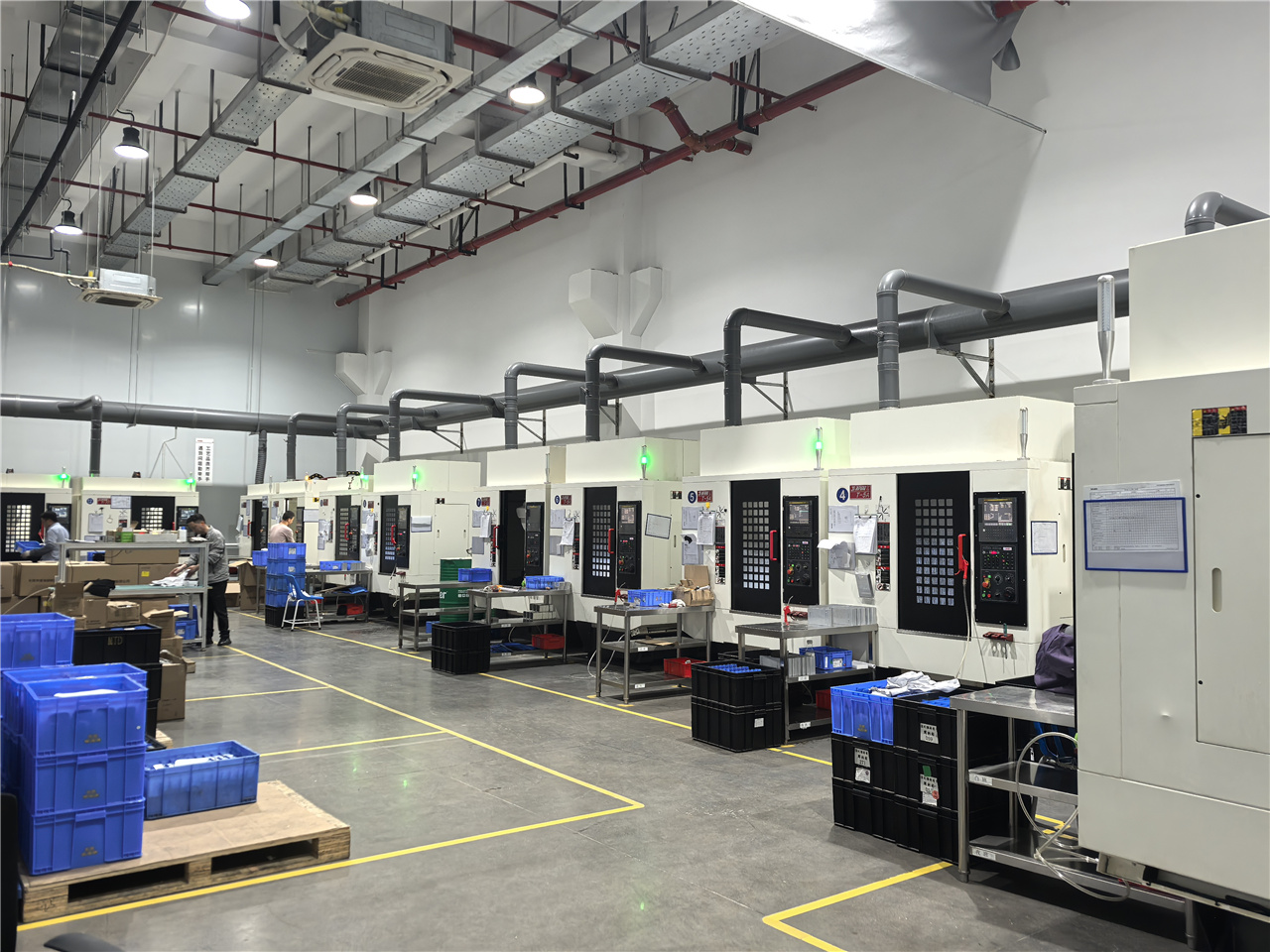
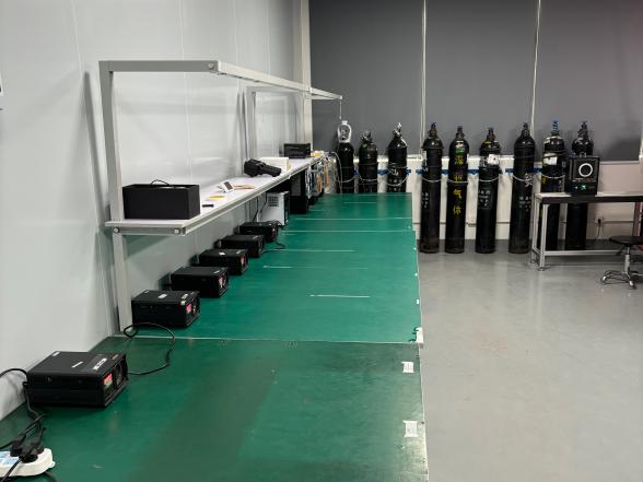
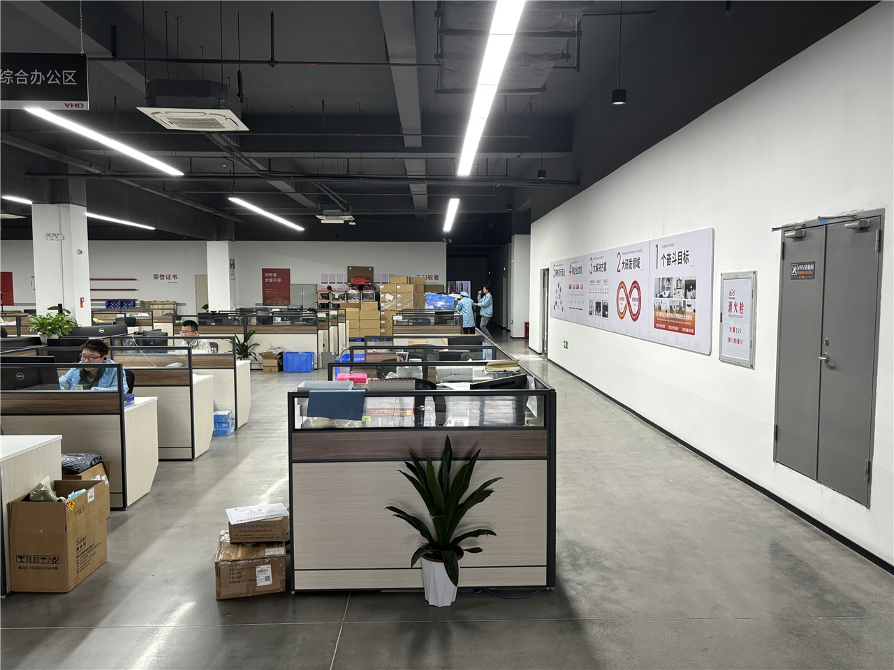
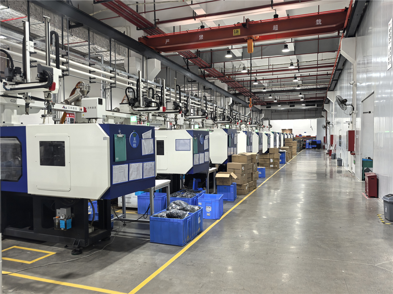
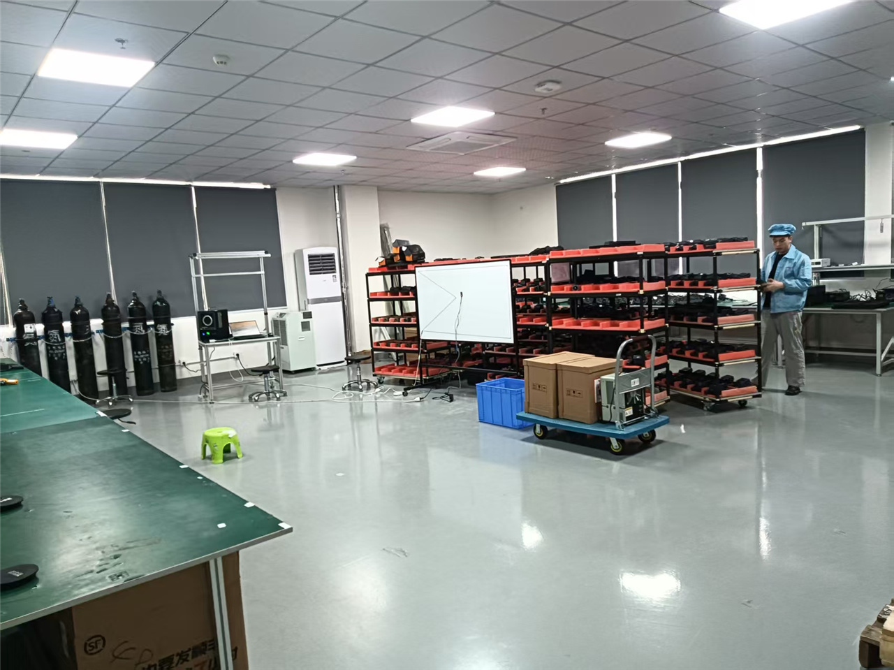
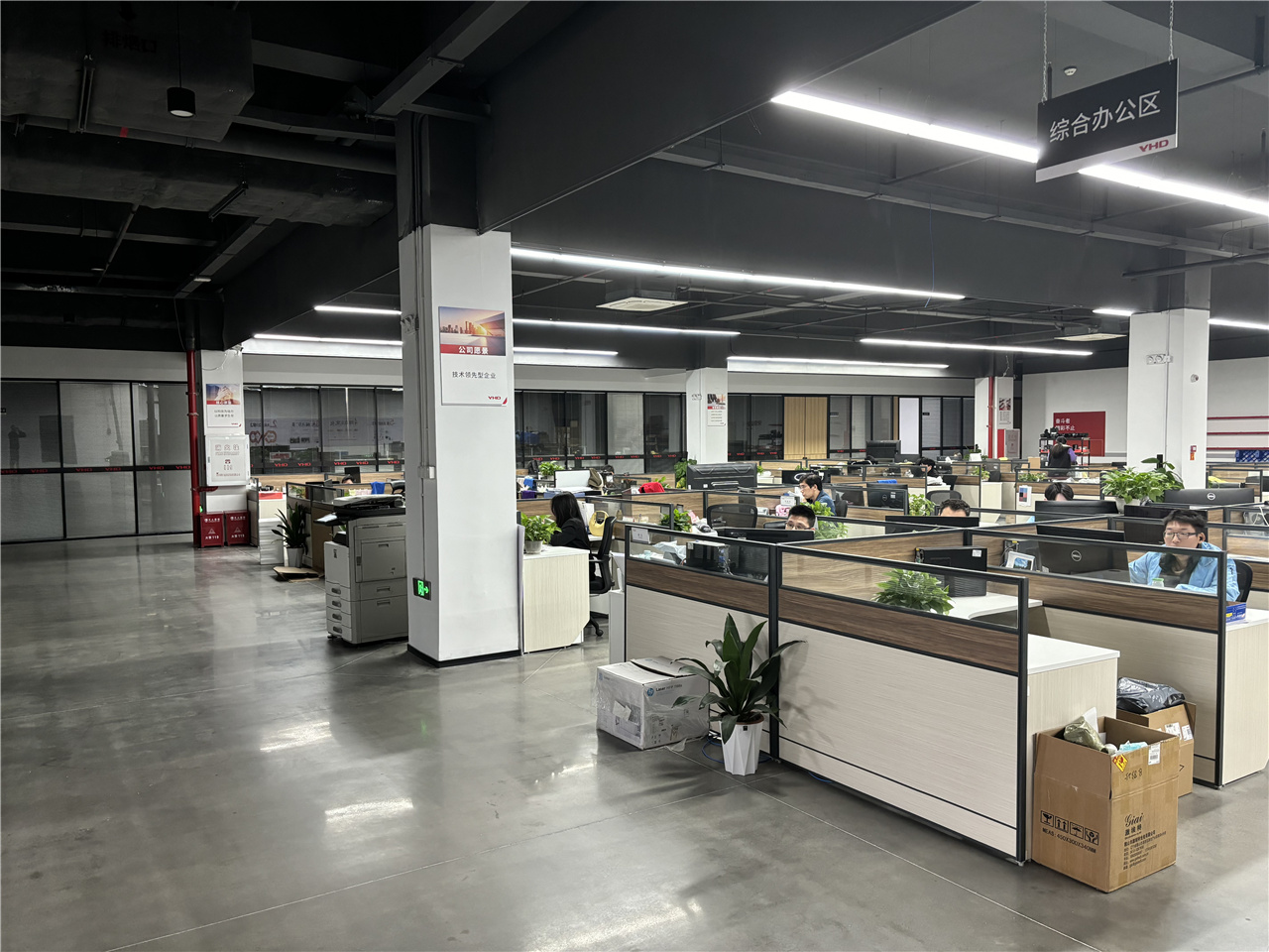
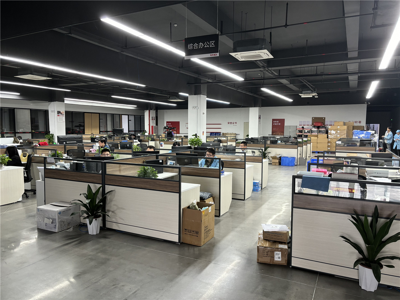
Delivering precision thermal optical products across international boundaries requires strict compliance with electrical, environmental, and optoelectronic standards. Shenzhen Dianyang Technology integrates rigorous end-to-end quality assurance (QA) mechanisms at every phase of OEM/ODM execution:
Technical guidance for optical engineers, procurement managers, and system integration specialists.
Select specialized infrared solutions engineered for industrial maintenance, mobile smartphone diagnostics, and customized thermal core integration.
 Dianyang